
This state-of-the-art technology has great advantages, and the future research trend is towards the application of 3D embedded electronics, 3D conformal electronics, flexible 3D printed electronics, and stretchable 3D printed electronics. An in-depth understanding of current developments in advanced functional materials and technologies for the fabrication of 3D printed electronics is warranted.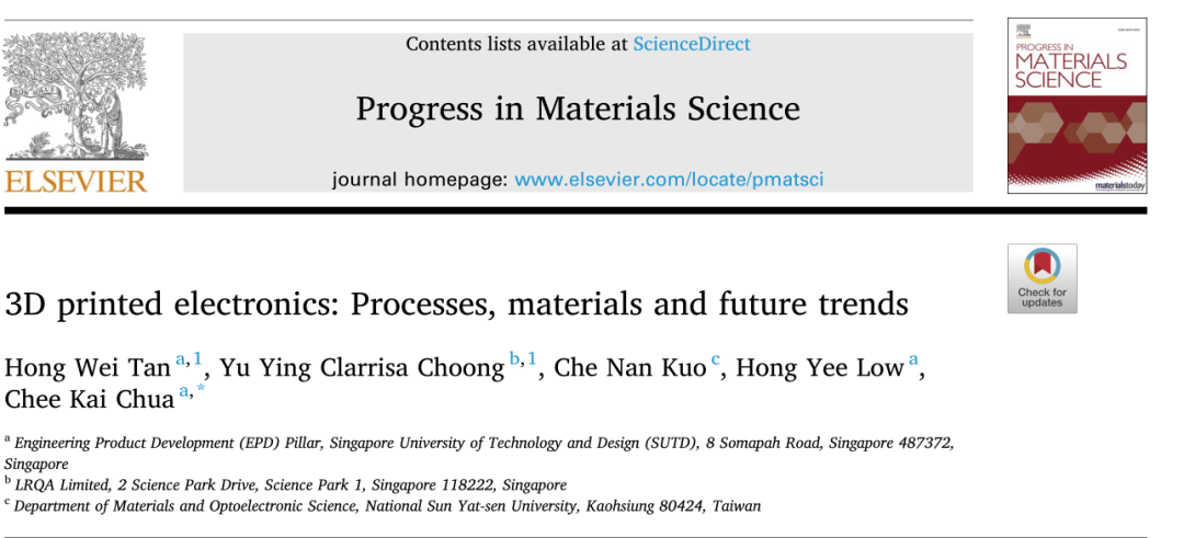
The Antarctic Bear learned that researchers from Singapore University of Science and Technology have sorted out the development and application of 3D printed electronic devices, and have published the research content in the journal “Progress in Materials Science”. An in-depth overview of technologies and innovative and practical techniques for fabricating 3D printed electronics is provided, and recent advances and future application trends of advanced functional materials for fabricating 3D printed electronics are discussed.
3D electronic printing technology
△ Classification of 3D electronic printing technology
3D electronic printing technology is defined as a printing technology that “deposits functional inks directly and precisely onto a substrate”. Among them, extrusion printing, inkjet printing, spray printing, and electrohydrodynamic (EHD) inkjet printing are the most widely used 3D printing techniques in the field of circuit 3D printing research, and these techniques can all be used to deposit functional inks directly onto substrates. on the material. According to the ISO/ASTM2021:52900 classification, extrusion printing can be classified as material extrusion, while inkjet printing, spray printing and electro-hydraulic jet printing can be classified as material jetting.
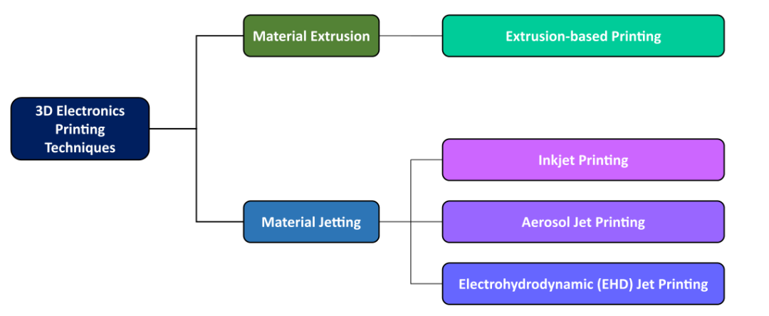
1. Extrusion printing
△ Extrusion printing schematic diagram
The principle of extrusion-based printing technology is simple and economical, in which a continuous flow of functional materials is achieved through nozzle extrusion. This technique can use a wider range of material viscosities and have fewer clogging issues than other printing techniques. However, this method is much slower and has poorer print resolution. Depending on the type of extruder used, extrusion-based printing can be further subdivided into filament-based extrusion, pneumatic-based extrusion, plunger-based extrusion, and screw-based extrusion. Pneumatic extrusion, ram extrusion and screw extrusion printing techniques are also collectively referred to as direct ink writing (DIW).
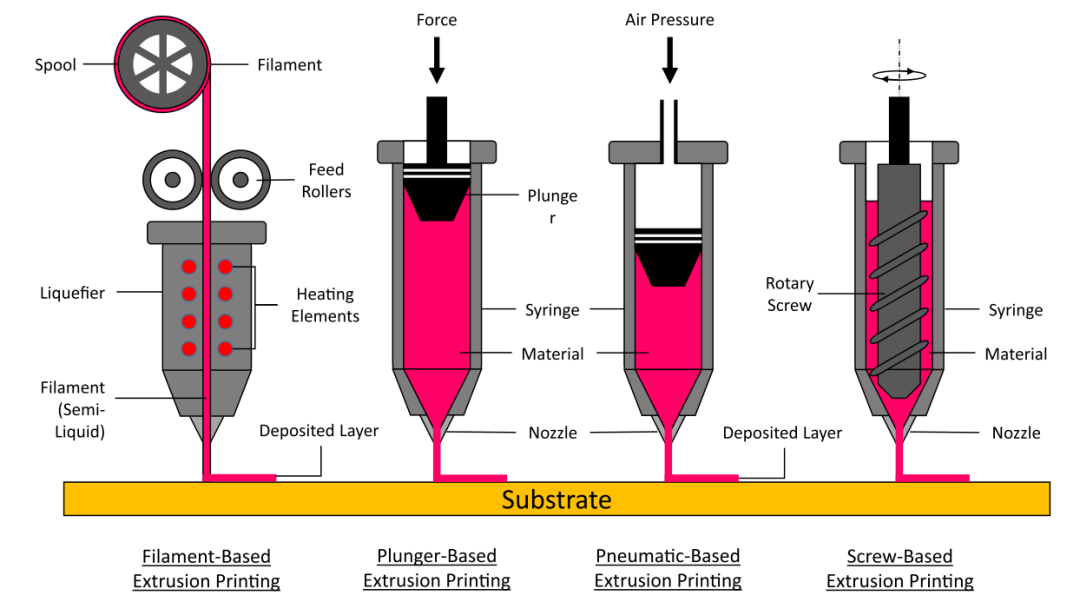
2. Inkjet printing
△ Schematic diagram of inkjet printing
Inkjet printing is a mature technology that has been widely used in many fields over the past few decades. It uses inkjet printing technology to build images by depositing ink onto a paper substrate. Using this technology, it is also possible to manufacture 3D printed electronics by depositing electrically functional and conductive materials. According to the droplet generation method, inkjet printing is divided into two categories: continuous inkjet printing (CIJ) and drop-on-demand printing (DoD). Generally speaking, inkjet printing technology is digital, non-contact, maskless and material saving. However, the inkjet printing technology generally faces the problem of nozzle clogging during the printing process. In addition to this, inkjet printing technology can only deposit low-viscosity fluids within a specific surface tension range. Thus, this limits the types of inks that can be deposited by inkjet printing. Inkjet printing technology is also generally not conducive to the deposition of functional materials onto non-planar surfaces.
3. Spray printing
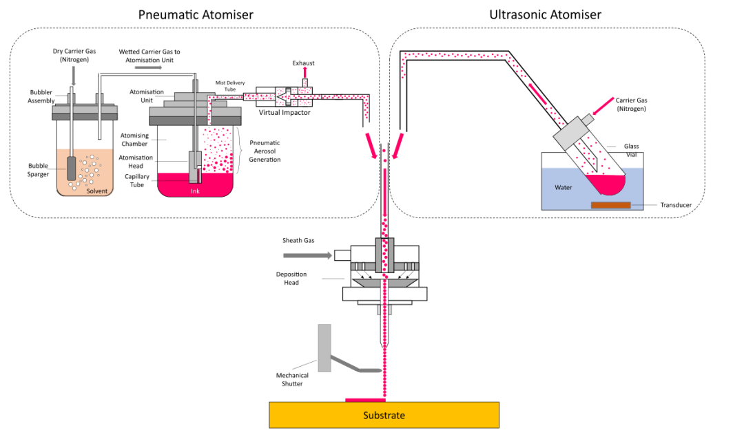
△ Schematic diagram of spray printing
Spray printing is an aerosol-based direct-write printing technique that produces a directional, collimated beam of aerosol for direct deposition of materials onto substrates. This technique is also known as aerodynamic focusing. Typically, spray printers are equipped with pneumatic or ultrasonic atomizers. Pneumatic atomizers can accept inks with viscosities ranging from 1 to 500cps, while ultrasonic atomizers can only accept inks with viscosities from 1 to 15cps. The aerosol jet process can deposit a range of functional materials for 3D printed electronic applications, including metallic nanoparticle inks, carbon nanotubes (CNTs), graphene, dielectric materials, and conducting polymers. Spray printers have demonstrated the ability to achieve print resolutions of 10 μm. Spray printing technology is also non-contact, reducing manufacturing contamination and damage.
4. Electro-Hydraulic Power (EHD) Injection
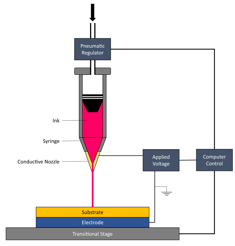
△ Schematic diagram of electro-hydraulic power (EHD) jet printing
In electro-hydraulic (EHD) inkjet printing, an electric field is used to create an electrical fluid in the process of creating a fluid flow. This usually requires high pressure to overcome the high capillary pressure in small nozzles, but this may not be technically feasible when the diameter of the nozzle is too small. Therefore, to overcome this problem, EHD inkjet printing technology works by applying an electric field rather than extracting ink from conductive nozzles. EHD jet printing technology can produce very fine lines and tiny droplets in the sub-micron range, and the inner diameter of the nozzle can be as small as 100nm. EHD jetting technology can deposit organic and inorganic materials for 3D printed electronic applications.
3D printing electronic functional materials
A large number of functional materials are used to make 3D printed electronic devices, and each type of material has its own unique function and purpose. In general, functional materials for 3D printed electronics can be classified into dielectric inks, metal nanoparticle inks, conductive polymers, metal organic decomposition (MOD) inks, carbon nanomaterial inks, and semiconductor inks.
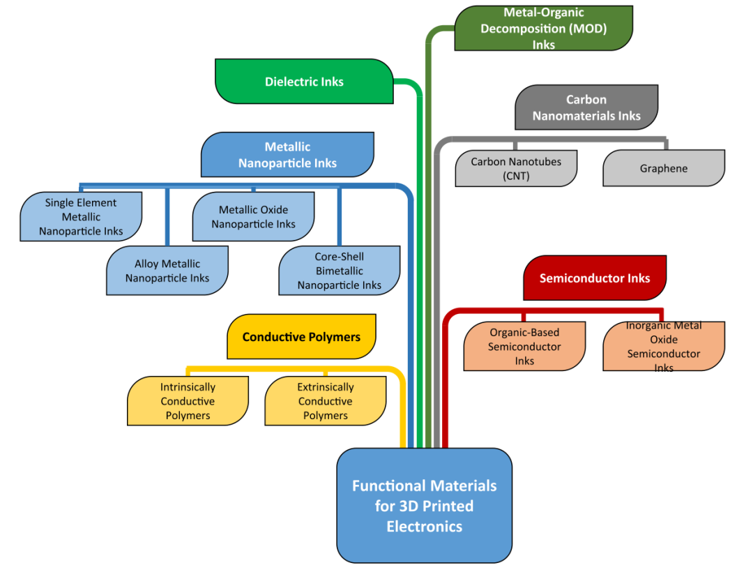
●Dielectric ink: Dielectric ink is an electrical insulating material. They play an important role in many aspects of 3D printed electronics, including circuit protection, multilayer circuit insulation, and the manufacture of capacitors and transistors.
●Metal nanoparticle ink: Metal nanoparticle ink is a suspension of conductive metal nanoparticles in liquid medium. Due to their good electrical conductivity, they are widely used in the fabrication of conductive traces and patterns in 3D printed electronic applications. A typical metal nanoparticle ink consists of three main components: metal nanoparticles, organic additives and stabilizers, and a liquid medium.
● Conductive polymers: Conductive polymers can be divided into intrinsic conductive polymers and extrinsic conductive polymers.
Metal organic decomposition (MOD) inks: Metal organic decomposition (MOD) inks are also known as metal organic inks, precursor type inks or inks that do not contain nanomaterials. MOD inks are highly concentrated metal-organic complexes or metal salts dissolved in organic solvents or aqueous solutions. They are also widely used in the fabrication of conductive traces and patterns in 3D printed electronics applications.
• Carbon Nanomaterial Inks: Carbon nanotubes (CNTs) are coiled graphene flakes with closed or open ends.
●Semiconductor inks: Semiconductor inks are used to manufacture 3D printed active electronic components. 3D printed active electronic components are often affected by properties such as the bandgap, on-off ratio, and mobility of the semiconductor ink. There are two main types of semiconductor inks, namely organic semiconductor inks and inorganic metal oxide semiconductor inks.
Trends in 3D printed electronics and materials
3D printing technology is expected to revolutionize and disrupt the current electronics industry in the near future. This new technology is designed to minimize time bottlenecks, waste and manufacturing costs, while allowing for highly innovative and on-demand manufacturing of customizable electronics in shorter prototyping times.
1. 3D printed electronics
●Flexible and stretchable 3D printed electronics
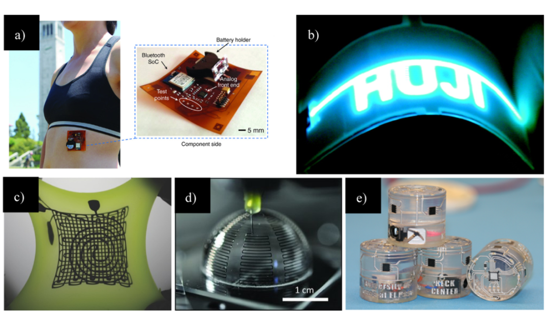
One of the current research trends is the move to flexible and stretchable 3D printed electronics. Such electronics could be used in many applications, especially in soft robotics and wearable healthcare monitoring. 3D printing technology can simply deposit functional materials directly onto flexible substrates. For many industry sectors, including healthcare and energy, flexible 3D printed electronics have the potential to provide more design freedom and reduce form factor constraints than traditional rigid electronics.
△Electronic devices
●Conformal electronics
Some 3D electronic printing technologies also allow the direct deposition of functional inks onto conformal surfaces to fabricate electronic devices on 3D surfaces. 3D conformal printing can enable more innovative designs and applications, while significantly reducing weight and making greater use of space. In addition, 3D conformal printing also takes form factor as a design consideration for making uniquely shaped antennas. Figure (d) above, shows a small antenna fabricated by directly depositing silver nanoparticle ink on the conformal surface of a hemispherical glass substrate.
●Embedded electronics
Some 3D electronic printing technologies also allow for multi-scale, multi-material and multifunctional printing. As a result, multifunctional structures or embedded electronics can be fabricated in a single print job, integrating conductive traces, active and passive components in complex non-planar geometries, see (e) above. Therefore, it is advantageous to save space, reduce weight, and protect components.
2. Materials
●Self-healing materials for flexible and stretchable electronic devices
Flexible and stretchable electronic devices can suffer mechanical damage from repeated bending and stretching, leading to device failure. Therefore, self-healing functional materials have received great attention in recent years. These materials inherently have the ability to repair damage automatically, and researchers are exploring their integration into flexible and stretchable electronic devices to increase the robustness of devices.
●Composite material
Composite materials are of increasing interest because of their improved ability to improve mechanical and electrical properties. In addition, composite materials allow the flexibility to tailor the desired electrical, mechanical and electromagnetic properties according to the needs of the application.
●4D printing materials
4D printing is a new field of 3D printing, which refers to the change of the shape, function and physical properties of 3D printed structures over time in response to external stimuli such as temperature differences, chemical reactions and optical illumination. For 4D printed electronics applications, conductive fillers can be incorporated into shape memory polymers (SMPS) to impart desired electrical properties. In addition to having conductive switching power supplies for 4D printed electronic applications, conductive functional materials can also be deposited directly on or embedded in 4D printed structures.
3D printed bioelectronic devices
Due to its ability to create highly integrated 3D multifunctional structures, many researchers are exploring this emerging technology to fabricate geometrically complex and biocompatible devices and scaffolds with electrical functions. Some of these devices include biosensors, electrically stimulating tissue regeneration scaffolds, and microelectrodes. A biosensor is a receptor that detects certain substances and responds to recognizable electrical signals. Electrical stimulation may also help promote faster regeneration of biological tissues. Therefore, several studies have been looking to integrate electronic devices into bioscaffolds to improve or enable regeneration processes.
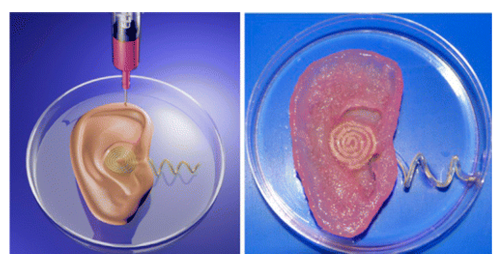
△ 3D printed a pair of left and right bionic ears, which can enhance the auditory perception of radio frequency reception and stereo audio music listening
●Biodegradable material
The most practical and attractive solution to the e-waste problem is to develop biodegradable electronic products, as biodegradability ensures that the waste generated is environmentally friendly and non-toxic. Therefore, it is of great significance to explore the use of biodegradable organic materials to fabricate biodegradable electronic devices. The efficiency and performance of such a device during operation is a key aspect that will determine the potential adoption of biodegradable 3D printed electronics. Materials require further research and development to accommodate the degradation times of various components for a variety of applications and requirements. Other important considerations include the effects of deformation due to cyclic mechanical loading and the reliability of biodegradable materials under operating pressures.
Summarize
Ideal functional inks for 3D printed electronic applications should have good material and electrical properties, good printability, cost-effectiveness, and the ability to withstand certain processing temperatures. The printing system must also have good print resolution, high print speed, on-demand non-contact printing, and allow for rapid design modification and easy expansion. To sustain the growth and adoption of 3D printed electronics, continued efforts in research and development of new advanced functional inks are required. It is necessary to develop various inks with different material properties, electronic properties and mechanical properties for various applications. Final electronic performance and print resolution are the two most important considerations for 3D printed electronics.
Ink manufacturers and machine builders are highly encouraged to collaborate and share their expertise to jointly formulate and optimize inks for a particular printer to better improve print suitability and print quality. It is believed that in the near future, the new 3D printing application of electronic products will realize its huge potential.


GIPHY App Key not set. Please check settings